
Research and Development

Building on its advanced technologies in photosensitive material development, Toyo Gosei is strengthening its collaborative systems and promoting future-oriented materials development.
 Executive Officer General Manager, Photosensitive Materials Research Center
Satoshi Enomoto We are leveraging the advanced technological capabilities honed through the development of our world-leading photosensitive materials to accelerate the development of valuable materials that meet market demand. This is made possible by going beyond the boundaries of our existing business and engaging in joint development with a variety of companies and research institutions in fields such as nanotechnology, life sciences, and energy. As a chemical manufacturer, we are also leveraging our long-standing development capabilities to develop PFAS-free materials and energy-saving technologies in order to realize a sustainable society. We will continue to strengthen our internal and external collaborative systems and promote value co-creation activities in fields where change and rapid progress are expected in the near future.
Market Environment
Our research and development mission is to connect innovation with everyday happiness through the power of materials. The Photosensitive Materials Research Center's goal is to develop and implement technologies to expand our business portfolio and strengthen our competitiveness in the rapidly advancing existing semiconductor materials business field by applying our synthesis and advanced purification technologies to new fields. Our basic policy for activities is to practice co-creation toward this goal.
Research and Development System
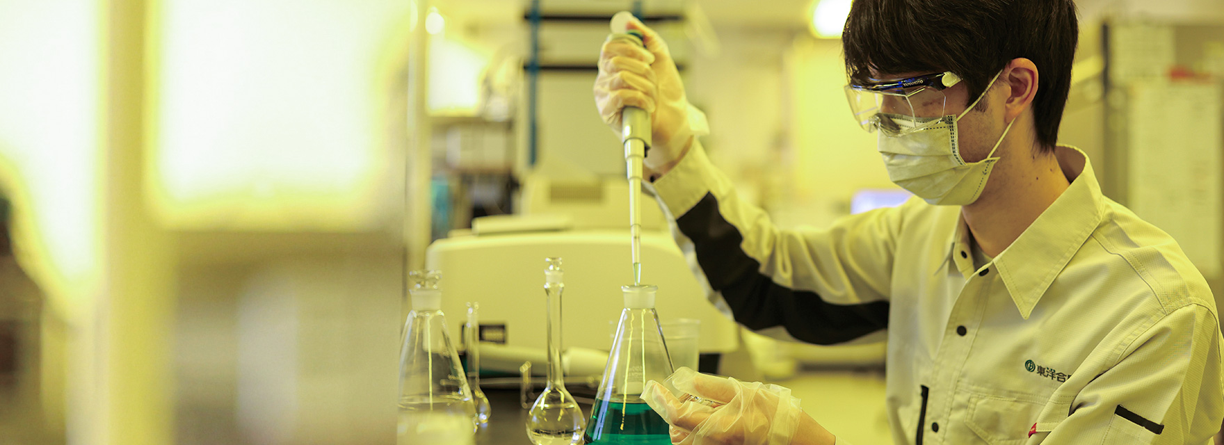
The Photosensitive Materials Research Center has established a specialized function-based organizational structure for development, consisting of a R&D planning department that manages planning for new business creation, a business development department responsible for business planning, commercialization, quality assurance, and business expansion, and multiple research and development departments that develop materials. Each department generates ideas that meet market needs and specialized personnel, who can conduct everything from material development to pilot production, work together to efficiently develop business and conduct research and development. Aiming to improve product quality, we are strengthening basic physical property evaluation and analysis in addition to developing instrumental analysis and analytical techniques. We are also working to speed up the improvement cycle by establishing a system for providing feedback on analytical data to the development and commercialization departments.
Strengths
・A development environment that enables us to proactively take on the challenge of approaching new business fields and creating new products and technologies based on the needs of today.
・Ability to apply our lineup of photosensitive materials and knowledge to photofunctional materials
・Purification technology and comprehensive analytical equipment to meet the cutting-edge needs of the semiconductor industry
Purification technology and comprehensive analytical equipment to meet the cutting-edge needs of the semiconductor industry
We are working on both organizational development and human resource development, seeking to become an organization that can analyze market needs and provide and commercialize developed products in a timely manner. As competition in development intensifies, we are also promoting the Digital Transformation (DX) of materials development. In order to develop and improve products using Material Informatics, we are working with external organizations to provide educational and practical opportunities. We are building our track record and data at actual development sites, and using this as a basis to improve our technical capabilities.
Furthermore, to advance our core technologies, we invite experts to our development projects as mentors, creating opportunities for discussion and learning using actual development cases, and working to solve problems and improve our technologies. This advances effective human resources development that utilizes action learning, where employees learn practically, in addition to regular on-the-job training (OJT) within the Company.
Approach to Intellectual Property
Toyo Gosei regards intellectual property as an important management resource that supports our future growth. We aim to appropriately protect and manage the outcomes of our research and development, leading to the long-term enhancement of our corporate value. We respect the intellectual property rights of other companies and strive to prevent infringements by thoroughly researching and analyzing existing technologies at each stage of product development. Furthermore, with regard to our own technological assets, we flexibly choose between acquiring rights through patent applications and keeping our know-how confidential, taking into account the risk of imitation and the market environment, thereby ensuring sustainable competitiveness and maintaining customer trust. In this way, we aim to promote research and development that strategically utilizes our intellectual assets.
Intellectual Property Management System
At Toyo Gosei, our intellectual property management section work closely with our research and development departments to oversee intellectual property-related matters. From identifying inventions and filing patent applications to maintaining and managing rights, our experienced staff consistently and properly oversee intellectual property matters, taking into account the technology and business policies. We also provide internal intellectual property consultations and technical reviews across the entire company, transcending the boundaries of our business locations, and we incorporate perspectives on intellectual property infringement risks and rights acquisition from the early stages of development. Furthermore, we collaborate with external patent attorneys and research organizations to establish a flexible and effective intellectual property management system, which protects our technological foundation and leads to continuous value creation.
Photosensitive Materials Research Center
Generating Value for the Future by Creating New Businesses and Strengthening Existing Businesses
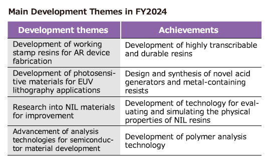
We have developed working stamp (WS) resins for AR*1 applications, which are photocurable resins for nanoimprint lithography (NIL) through proactive alliances both internally and externally, and have received high praise from users. In the application development of photosensitive materials, we are also developing new materials for cutting-edge EUV*2 applications. Toward these new developments and the growth of our existing businesses, we are establishing a development system featuring evaluation and analysis technology, disseminating outcomes, and contributing to the development of society and the Company through the improvement of our development capabilities.
※1. AR(Augmented Reality) is a technology that extends reality by overlaying digital information on the real world.
2. EUV (Extreme Ultraviolet) is an extreme ultraviolet light, a cutting-edge lithography technology used to form the smallest circuit structures in semiconductors.
TOPICS
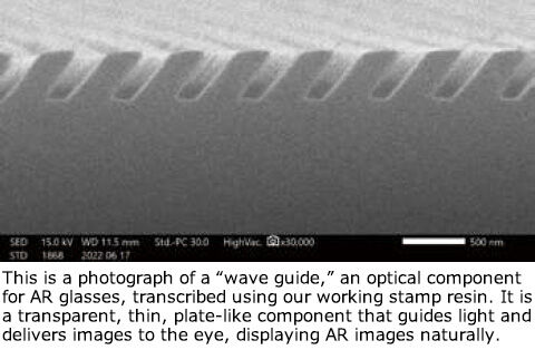
Development of WS Resin Molds that Meet Market and Customer Expectations
NIL technology is being explored for the manufacture of optical components such as AR glasses (eyeglass-type devices), a market expected to grow in the future. NIL technology typically involves creating an expensive, precise master mold and then using a working stamp resin mold replicated from that master mold, which requires high-precision replication. Our working stamp resin hardens solely through a UV exposure process, replicating the shape of the master mold exactly without the need for heat treatment or other processes for removal from the mold. Furthermore, because its shape and size do not change even with repeated use, it allows for the mass production of stable, high-quality products and improves production efficiency. This has led many companies to consider adopting our working stamp resin.
- Message from CEO
-
TOYO GOSEI REPORT2025 DOWNLOAD
(Japanese version only) - Toyo Gosei Co., Ltd. in Our Lives
- Toyo Gosei's Business and Sustainability
- Safety Initiatives
- Human Capital Initiatives
- Initiatives for Respecting Human Rights
- Social and Environmental Initiatives
- Initiatives for Business Continuity
- Initiatives for Sound
Corporate Management - Research and Development
- Sustainability Data