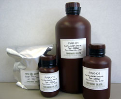
UV nanoimprint resin PAK-01*
*Our UV nanoimprint resins are products under development.
Photocurable resin PAK-01 is the first resin dedicated to UV nanoimprint (UV-NIL) in Japan. This product is optimized for UV nanoimprint and is widely used in research and development.
Features of PAK-01
Applicability: High spin-coat applicability, applicable to large areas
Releasability: High releasability, minimal damage to mold
Transferability: Transfer of minimum 20nm is possible (actual value of PAK-01)
Properties of PAK-01
Appearance: Transparent viscous liquid
Kinematic viscosity: 50 to 65 cSt (about 60 mPa · sec)
Recommended exposure: 10mJ / cm2 or more
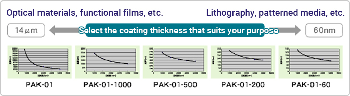
UV nanoimprint resin PAK-01 lineup
A wide lineup according to the film thickness is available to support various applications and processes. You can consider the film thickness from 14 microns to 60 nanometers.
Results of use of PAK-01 resin for UV nanoimprint and research example
UV nanoimprint resin PAK-01 is widely used in research institutes in Japan and overseas, and is highly evaluated as a test resin. The process margin is wide because it does not depend on the material of the substrate or the mold to be used, and it can support many engineering processes. It is examined a wide range of research fields, such as high aspect ratio transfer and initial examination of dry etching process.
Waseda University
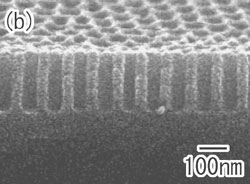
 Processing example of Si substrate
By using the PAK-01 pattern for UV nanoimprint resin as a resist, Si processing by dry etching is possible. In order to accurately control the thickness of the remaining film, a thin-film coating type PAK-01 is used.
AIST, Tokyo University of Science
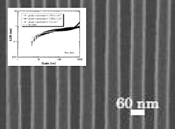 Research example of nanoimprint resolution
The patterning accuracy of nanoimprint was examined based on the LER (line edge roughness) value of the UV nanoimprint resin PAK-01, and proved to be overwhelmingly better than other processing technologies (such as semiconductor lithography).
Tokyo Metropolitan University
 Research example of high aspect patterning
We manufacture molds with high aspect nano patterns and transfer them to UV nanoimprint resin PAK-01. Even in the case of such a high aspect transfer, pattern collapse does not occur.
UV nanoimprint resin PAK-02*
*Our UV nanoimprint resins are products under development.
PAK-02 is a UV nanoimprint resin developed for optical components. This product is suitable for mass production test using roll imprinting equipment.
Features of PAK-02
- Optimal for optical applications/production tests
- transparency
- Adhesion to organic substrates
- Releasability from metal mold
Properties of PAK-02
- Appearance ・ ・ ・ ・ Transparent viscous liquid
- Viscosity ・ ・ ・ ・ ・ ・ 9 mPa ・ sec
- Recommended light source: Ultra-high pressure mercury lamp, UV-LED, metal halide lamp, etc.
- Refractive index
(D line: 589 nm, after UV curing) ・ ・ ・ 1.51
Permeability of PAK-02 (comparison with PAK-01)
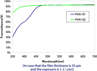
Performance comparison between PAK-01 and PAK-02
UV nanoimprinting resin PAK-02 enables imprinting on Ni molds and resin substrates while maintaining the excellent features of PAK-01 (release, adhesion, and applicability). Also, since the cured film is transparent, it is the best option as an optical materials.
| item | Material | PAK-01 | PAL-02 |
|---|---|---|---|
| Coating and adhesion | Inorganic substrate (Si, etc.) | ○ | × |
| Organic substrate (PC, TAC, etc.) | △ | ○ | |
| Mold release | Quartz mold (with release treatment) | ○ | ○ |
| Ni mold (without release treatment) | △ | ○ | |
| Non-coloring (400nm ~) | △ | ○ |
Pak-02 UV Nanoimprint Resin usage record and research example
UV nanoimprinting resin PAK-02 is suitable for large area transfer with roll imprinting equipment and we have abundant test results in the equipment. The application properties, mold release properties, and board adhesiveness required as basic resin properties vary greatly depending on the board and mold material used.PAK-02 has excellent adhesion to organic substrates and releasability from metal molds, and has a good process margin.
Example of large area transfer by roll imprinting machine. Toshiba Machine-Roll-to-roll fine transfer machine
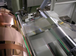 The pattern was transferred to the film substrate using a roll-shaped metal mold. It has few process errors even in actual machine tests, and is suitable for large area transfer.
Example of V-groove shape transfer photo provided by Toshiba Machine
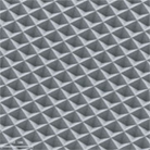 This is a micro-sized V-groove shape transferred onto a film using a roll-imprinter. It shows good transferability with few defects.
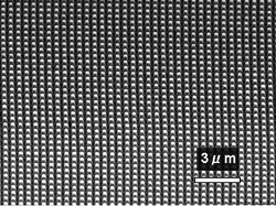
Example of fine pattern transfer
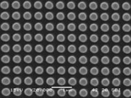 UV nanoimprint resin PAK-02 has good nano-order pattern transferability. Here is an example of a 300nm dot pattern transfer.
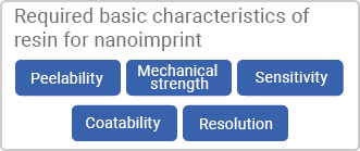
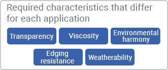
Required properties for UV nanoimprint resin
The required properties of UV nanoimprint resins can be broadly divided into (1) UV nanoimprint (UV-NIL) process characteristics, which are common regardless of the application, and (2) application-specific characteristics, which differ for each application. UV nanoimprint process characteristics include substrate adhesion, mold release, rapid curing, and mechanical strength. In addition to these properties, we are developing high-performance resins with properties tailored to each application.
Changes in film thickness due to process differences
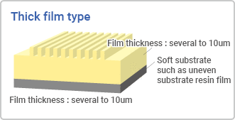
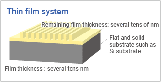
Required properties of resin (common properties and properties for each application)
Examples of development of UV nanoimprint resin by application
For dry process
 Required characteristics
Dry etching resistance, thin film transferability
Test example
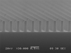
1. Patterning of dry etching resin by UV nanoimprint (UV-NIL)
2.Removal of residual film of resin pattern
3.Process the substrate by dry etching using the obtained resin pattern as a mask
The photo on the right shows a 140-nm pillar-shaped Si pattern produced by this process.
For wet process
 Required characteristics
Liquid resistance, dry etching resistance, thin film transfer property
Test example
1. Patterning of wet process resin by UV nanoimprint (UV-NIL)
2.Removal of residual film of resin pattern
3.Electroforming using the obtained pattern as a mask
4.Process the substrate by dry etching using the electroformed pattern as a mask
The photo on the right shows a GaN pattern with a 500nm pitch uneven shape produced by
the same process.
For permanent materials
 Required characteristics
Weather resistance, moisture resistance, heat resistance, non-coloring, etc.
Required physical properties differ for each target device.
Test example
1. Coating resin for optical parts on film
2.Contact Ni mold and resin
3. Release after exposure from substrate side
The photo on the right shows a resin film that has been transferred in a batch of 8 inches φ by the same process.